

Qualcomm Validates HBC Silicon With Huge 18x Leap In AI Memory Bandwidth
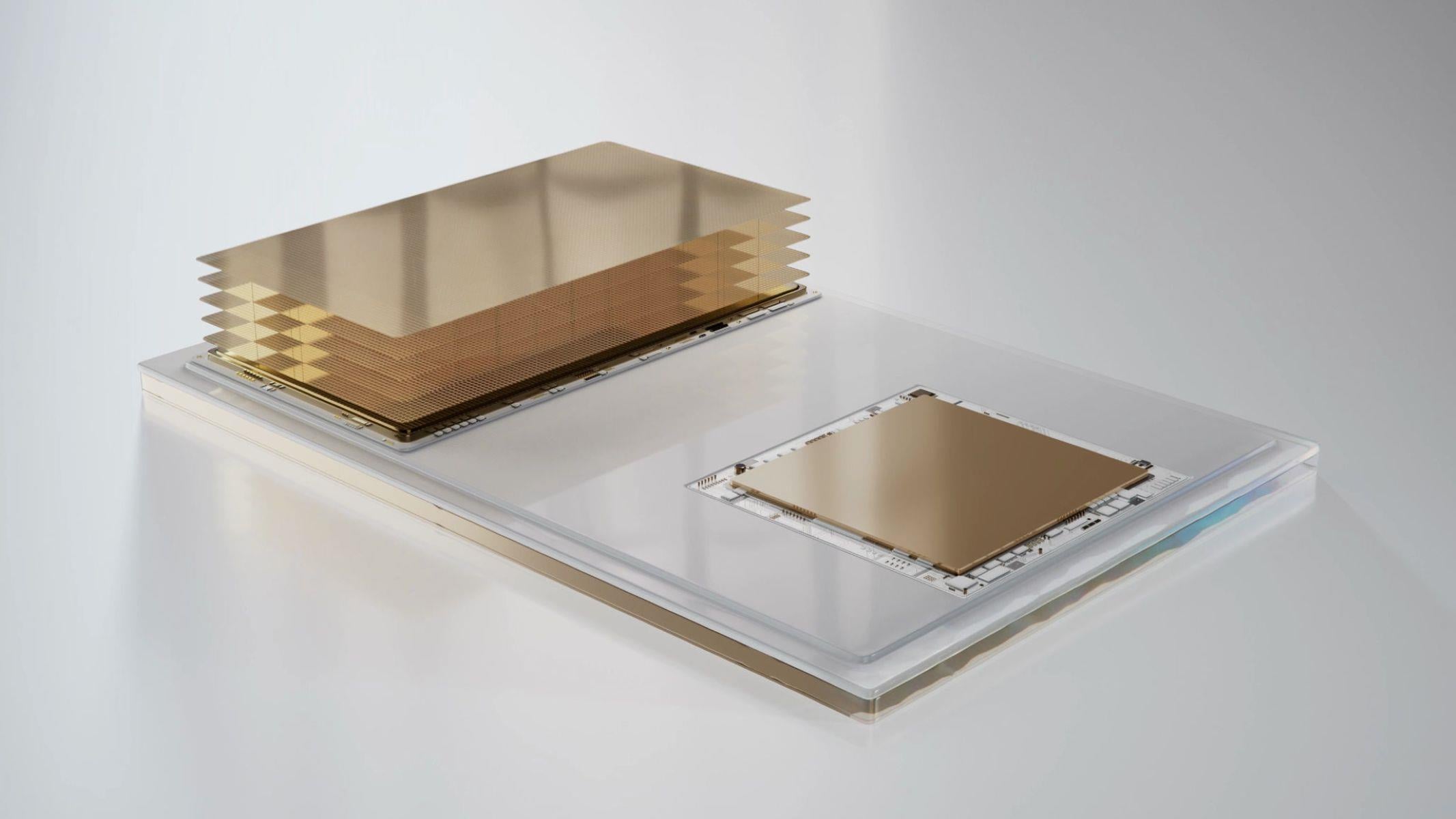
Qualcomm has announced validation its first-generation High Bandwidth Compute (HBC) silicon in the company's San Diego labs, with testing showing 18 times greater bandwidth over DDR5 and five times the efficiency of HBM4.
Computing demands have been changing as LLMs transition from training to large-scale agentic inference, specifically how the latter is bound primarily by memory bandwidth, or rather, how rapidly weight and activation data can traverse the physical space between memory pools and processing units. While high bandwidth memory (HBM) is the current go-to solution, HBM incurs steep thermal, financial, and electrical power premiums due to off-package data movement over millimeter distances. SRAM-based alternatives offer massive throughput but falter on memory capacity and total cost of ownership at rack scale.
Enter Qualcomm's HBC architecture, which vertically stacks low-power LPDDR memory dies directly on top of an active AI accelerator base die using direct wafer-to-wafer bonding. By shifting data...
Copyright of this story solely belongs to hothardware.com. To see the full text click HERE