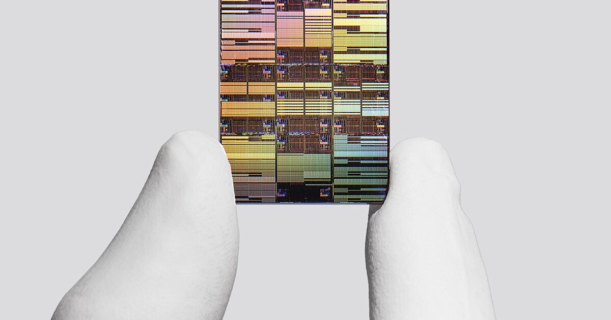
IBM's fingernail-sized chip squeezes in ~100 billion transistors
June 26, 2026
IBM's sub-1-nanometer node chip fits close to 100 billion transistors for increased efficiency and performance over the 2-nm process node
View 3 Images
IBM has developed the blueprint for producing a processor using sub-1-nanometer (nm) chip technology, outdoing its own efforts to increase efficiency and processing power with 2-nm tech from a few years ago.
The 1-nm figure isn't really an accurate measure of the size of transistors anymore. That part of the name of a process node (or chip manufacturing technique) used to refer to the physical gate length of a transistor.
This brief video below explains how that's changed over the years. The key takeaway is that transistors are now three-dimensional and can't be measured the same way as previous generations. What is a lot more important now is transistor density, or how many chips you can fit on to...
Copyright of this story solely belongs to newatlas.com. To see the full text click HERE