
ASML, TSMC, And Samsung Team Up To Solve Next-Gen Chip Bottleneck

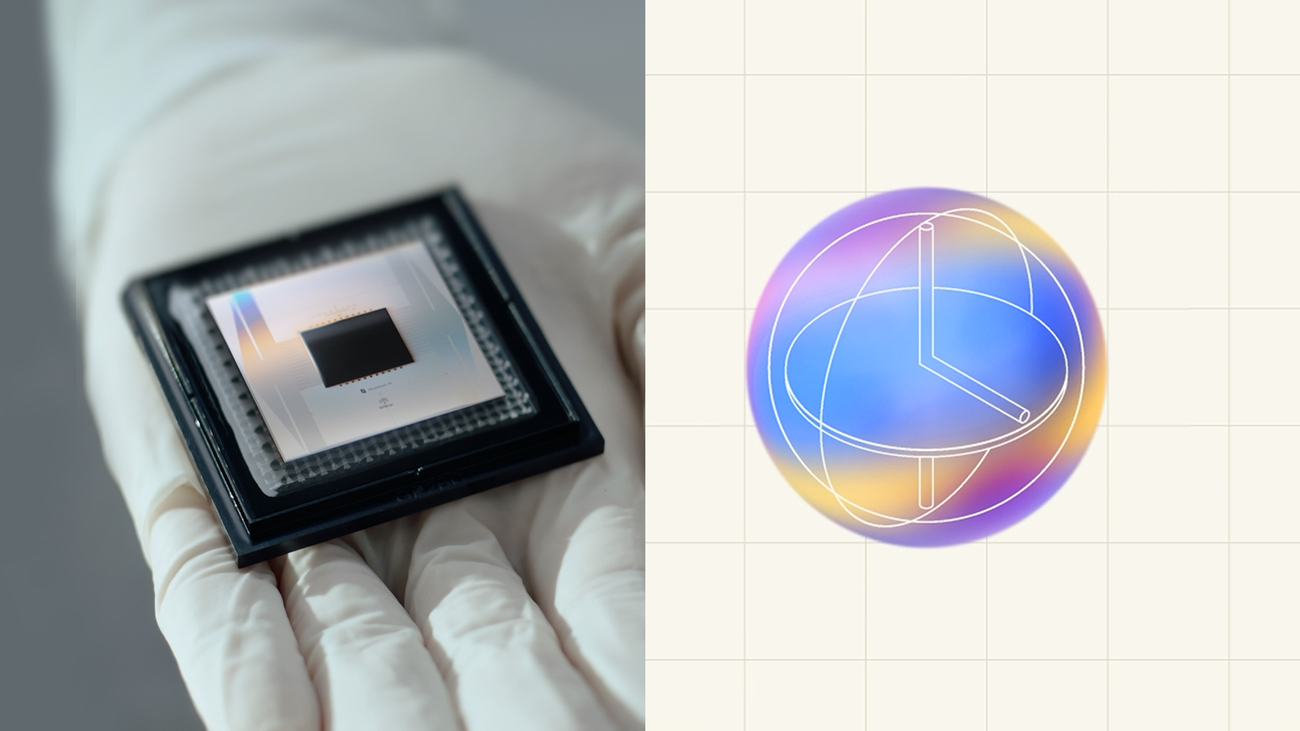
The semiconductor industry is entering a new phase as Samsung and TSMC commit to integrating ASML’s next-generation High Numerical Aperture Extreme Ultraviolet (High NA EUV) lithography into their manufacturing toolkits. To unleash the technology's full capability, these industry leaders are spearheading a joint shift toward larger, 12-inch photomasks.
For years, the extreme cost (estimated at upwards of $350 million per scanner) and unique engineering made chipmakers cautious about jumping straight into High NA EUV. However, the demand for advanced artificial intelligence hardware and shrinking transistor limits have forced their hand. Following early adoption by Intel, Samsung has announced plans to deploy ASML’s High NA EUV tools into high-volume manufacturing by 2028, targeting its advanced DRAM memory nodes to become the first memory maker to utilize the technology at scale. TSMC, the world’s largest contract foundry, also confirmed it will incorporate High NA EUV machines into its high-volume advanced node...
Copyright of this story solely belongs to hothardware.com. To see the full text click HERE